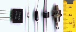
Types of diodes
In electronics, a diode is a component that restricts the direction of movement of charge carriers. It allows an electric current to flow in one direction, but essentially blocks it in the opposite direction. Thus the diode can be thought of as an electronic version of a check valve.
The first diodes were vacuum tube devices (called valves in the UK), but today the most common diodes are made from ultrapure semiconductor materials such as silicon or germanium.
The term was coined by William Henry Eccles in 1919 from Greek roots; di means 'two', and ode means 'path'.
Thermionic or gaseous state diodes[]
The first diodes were vacuum tube devices (also known as thermionic valves), arrangements of electrodes surrounded by a vacuum within a glass envelope, similar in appearance to incandescent light bulbs. The arrangement of a filament and plate as a diode was invented in 1904 by John Ambrose Fleming (scientific adviser to the Marconi Company) based on an observation by Thomas Edison.
In vacuum tube diodes, a current is passed through the cathode, a filament treated with a mixture of barium and strontium oxides, which are rare earth metals. The current heats the filament, causing thermionic emission of electrons into the vacuum envelope. In forward operation, a surrounding metal electrode, called the anode, is positively charged, so that it electrostatically attracts the emitted electrons. However, electrons are not easily released from the unheated anode surface when the voltage polarity is reversed and hence any reverse flow is a very small current.
For much of the 20th century vacuum tube diodes were used in analog signal applications, and as rectifiers in power supplies. Today, tube diodes are only used in niche applications, such as rectifiers in tube guitar and hi-fi amplifiers, and specialized high-voltage equipment.
Semiconductor diodes[]
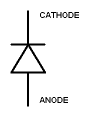
Most modern diodes are based on semiconductor p-n junctions. In a p-n diode, conventional current can flow from the p-type side (the anode) to the n-type side (the cathode), but not in the opposite direction. Another type of semiconductor diode, the Schottky diode, is formed from the contact between a metal and a semiconductor rather than by a p-n junction.
A semiconductor diode's current-voltage, or I-V, characteristic curve is ascribed to the behavior of the so-called depletion layer or depletion zone which exists at the p-n junction between the differing semiconductors. When a p-n junction is first created, conduction band (mobile) electrons from the N-doped region diffuse into the P-doped region where there is a large population of holes (places for electrons in which no electron is present) with which the electrons "recombine". When a mobile electron recombines with a hole, the hole vanishes and the electron is no longer mobile. Thus, two charge carriers have vanished. The region around the p-n junction becomes depleted of charge carriers and thus behaves as an insulator. However, the depletion width cannot grow without limit. For each electron-hole pair that recombines, a positively-charged dopant ion is left behind in the N-doped region, and a negatively charged dopant ion is left behind in the P-doped region. As recombination proceeds and more ions are created, an increasing electric field develops through the depletion zone which acts to slow and then finally stop recombination. At this point, there is a 'built-in' potential across the depletion zone. If an external voltage is placed across the diode with the same polarity as the built-in potential, the depletion zone continues to act as an insulator preventing a significant electric current. However, if the polarity of the external voltage opposes the built-in potential, recombination can once again proceed resulting in substantial electric current through the p-n junction. For silicon diodes, the built-in potential is approximately 0.6 V. Thus, if an external current is passed through the diode, about 0.6 V will be developed across the diode such that the P-doped region is positive with respect to the N-doped region and the diode is said to be 'turned on'.
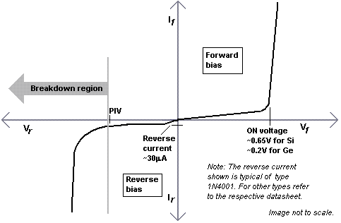
I-V characteristics of a P-N junction diode (not to scale).
A diode's I-V characteristic can be approximated by two regions of operation. Below a certain difference in potential between the two leads, the depletion layer has significant width, and the diode can be thought of as an open (non-conductive) circuit. As the potential difference is increased, at some stage the diode will become conductive and allow charges to flow, at which point it can be thought of as a connection with zero (or at least very low) resistance. More precisely, the transfer function is logarithmic, but so sharp that it looks like a corner on a zoomed-out graph (see also signal processing).
The Shockley ideal diode equation (named after William Bradford Shockley) can be used to approximate the p-n diode's I-V characteristic.
- ,

where I is the diode current, IS is a scale factor called the saturation current, q is the charge on an electron (the elementary charge), k is Boltzmann's constant, T is the absolute temperature of the p-n junction and VD is the voltage across the diode. The term kT/q is the thermal voltage, sometimes written VT, and is approximately 26 mV at room temperature. n (sometimes omitted) is the emission coefficient, which varies from about 1 to 2 depending on the fabrication process and semiconductor material.
It is possible to use shorter notation. Putting

and the relationship of the diode becomes:


where (at room temperature) is a known constant.

In a normal silicon diode at rated currents, the voltage drop across a conducting diode is approximately 0.6 to 0.7 volts. The value is different for other diode types - Schottky diodes can be as low as 0.2 V and light-emitting diodes (LEDs) can be 1.4 V or more depending on the current.
Referring to the I-V characteristics image, in the reverse bias region for a normal P-N rectifier diode, the current through the device is very low (in the µA range) for all reverse voltages upto a point called the peak-inverse-voltage (PIV). Beyond this point a process called reverse breakdown occurs which causes the device to be damaged along with a large increase in current. For special purpose diodes like the avalanche or zener diodes, the concept of PIV is not applicable since they have a deliberate breakdown beyond a known reverse current such that the reverse voltage is "clamped" to a known value (called zener voltage). The devices however have a maximum limit to the current and power in the zener or avalanche region.
Types of semiconductor diode[]
There are several types of semiconductor junction diodes:
- Normal (p-n) diodes
- which operate as described above. Usually made of doped silicon or, more rarely, germanium. Before the development of modern silicon power rectifier diodes, cuprous oxide and later selenium was used; its low efficiency gave it a much higher forward voltage drop (typically 1.4-1.7V per "cell," with multiple cells stacked to increase the peak inverse voltage rating in high voltage rectifiers), and required a large heat sink (often an extension of the diode's metal substrate), much larger than a silicon diode of the same current ratings would require.
- 'Gold doped' diodes
- The gold causes 'minority carrier suppression.' This lowers the effective capacitance of the diode, allowing it to operate at signal frequencies. A typical example is the 1N914. Germanium and Schottky diodes are also fast like this, as are bipolar transistors 'degenerated' to act as diodes. Power supply diodes are made with the expectation of working at a maximum of 2.5 x 400 Hz (sometimes called 'French power' by Americans), and so are not useful above a kilohertz.
- Zener diodes (pronounced /ziːnər/)
- diodes that can be made to conduct backwards. This effect, called Zener breakdown, occurs at a precisely defined voltage, allowing the diode to be used as a precision voltage reference. In practical voltage reference circuits Zener and switching diodes are connected in series and opposite directions to balance the temperature coefficient to near zero. Some devices labeled as high-voltage Zener diodes are actually avalanche diodes (see below). Two (equivalent) Zeners in series and in reverse order, in the same package, constitute a transient absorber (or Transorb, a registered trademark). They are named for Dr. Clarence Melvin Zener of Southern Illinois University, inventor of the device.
- Avalanche diodes
- diodes that conduct in the reverse direction when the reverse bias voltage exceeds the breakdown voltage. These are electrically very similar to Zener diodes, and are often mistakenly called Zener diodes, but break down by a different mechanism, the avalanche effect. This occurs when the reverse electric field across the p-n junction causes a wave of ionization, reminiscent of an avalanche, leading to a large current. Avalanche diodes are designed to break down at a well-defined reverse voltage without being destroyed. The difference between the avalanche diode (which has a reverse breakdown above about 6.2 V) and the Zener is that the channel length of the former exceeds the 'mean free path' of the electrons, so there are collisions between them on the way out. The only practical difference is that the two types have temperature coefficients of opposite polarities.
- Transient voltage suppression (TVS) diodes
- These are avalanche diodes designed specifically to protect other semiconductor devices from electrostatic discharges. Their p-n junctions have a much larger cross-sectional area than those of a normal diode, allowing them to conduct large currents to ground without sustaining damage.
- Photodiodes
- Semiconductors are subject to optical