(Copy from Wikipedia- edited - images uploaded) |
No edit summary Tag: rte-wysiwyg |
||
| Line 3: | Line 3: | ||
=== Basic logic gates and mechanical equivalents === |
=== Basic logic gates and mechanical equivalents === |
||
| − | While [[semiconductor]] electronic logic (see later) is preferred in most applications, relays and [[switch]]es are still used in some industrial applications and for educational purposes. |
+ | While [[semiconductor]] electronic logic (see later) is preferred in most applications, relays and [[switch]]es are still used in some industrial applications and for educational purposes. In this article, the various types of logic gates are illustrated with drawings of their relay-and-switch implementations, although the reader should remember that these are electrically different from the semiconductor equivalents that are discussed later. |
| − | Relay logic was historically important in industrial automation (see [[ladder logic]] and [[programmable logic controller]]). Since relay contacts conduct in both directions, complex logic designs must be checked for "sneak paths" that produce unintended logic paths. |
+ | Relay logic was historically important in industrial automation (see [[ladder logic]] and [[programmable logic controller]]). Since relay contacts conduct in both directions, complex logic designs must be checked for "sneak paths" that produce unintended logic paths. |
Semiconductor logic gates are ''not'' conductive in both directions, as the input signal acts as a 'trigger' to allow current out of the output, rather than allowing current straight through from input to output. However, the following mechanical variations do show the basic principles of the gates without detailing the precise internal workings. For information about how modern semiconductors really work, see [[CMOS]]. |
Semiconductor logic gates are ''not'' conductive in both directions, as the input signal acts as a 'trigger' to allow current out of the output, rather than allowing current straight through from input to output. However, the following mechanical variations do show the basic principles of the gates without detailing the precise internal workings. For information about how modern semiconductors really work, see [[CMOS]]. |
||
| Line 13: | Line 13: | ||
==== AND gates ==== |
==== AND gates ==== |
||
| − | The first example is the [[logical conjunction|AND]] gate, whose [[truth table]] is shown below, left. The Boolean AND function can be implemented with two switches, A and B, as shown below, right. |
+ | The first example is the [[logical conjunction|AND]] gate, whose [[truth table]] is shown below, left. The Boolean AND function can be implemented with two switches, A and B, as shown below, right. If a power lead is connected to switch A, and a wire connects switches A and B, then both A and B have to be "on" in order for the output of the circuit to conduct electricity and provide power. |
| − | <table align="left" width="20%" border="1" style="float:left"> |
+ | <table align="left" width="20%" border="1" style="float:left"><tr bgcolor="#ddeeff" align="center"> |
| ⚫ | |||
<th colspan="2">INPUT</th> |
<th colspan="2">INPUT</th> |
||
| − | <th>OUTPUT</th> |
+ | <th>OUTPUT</th></tr><tr bgcolor="#ddeeff" align="center"> |
| ⚫ | |||
<td>A</td> |
<td>A</td> |
||
<td>B</td> |
<td>B</td> |
||
<td>A AND B</td> |
<td>A AND B</td> |
||
| + | </tr> |
||
<tr bgcolor="#ddffdd" align="center"> |
<tr bgcolor="#ddffdd" align="center"> |
||
<td>0</td> |
<td>0</td> |
||
<td>0</td> |
<td>0</td> |
||
| ⚫ | |||
| ⚫ | |||
| ⚫ | |||
<td>1</td> |
<td>1</td> |
||
<td>0</td> |
<td>0</td> |
||
| ⚫ | |||
| − | <td>0</td> |
||
| ⚫ | |||
<td>0</td> |
<td>0</td> |
||
<td>1</td> |
<td>1</td> |
||
| ⚫ | |||
| − | <td>0</td> |
||
| ⚫ | |||
<td>1</td> |
<td>1</td> |
||
<td>1</td> |
<td>1</td> |
||
| − | <td>1</td> |
+ | <td>1</td></tr></table> |
| − | </table> |
||
[[Image:circuit and.png|right|frame|Switch circuit diagram for AND gate]] |
[[Image:circuit and.png|right|frame|Switch circuit diagram for AND gate]] |
||
| Line 65: | Line 60: | ||
| − | <table align="" width="20%" border="1" style="float:left"> |
+ | <table align="" width="20%" border="1" style="float:left"><tr bgcolor="#ddeeff" align="center"> |
| ⚫ | |||
<th width="66%" colspan="2">INPUT</th> |
<th width="66%" colspan="2">INPUT</th> |
||
| − | <th width="33%">OUTPUT</th> |
+ | <th width="33%">OUTPUT</th></tr><tr bgcolor="#ddeeff" align="center"> |
| ⚫ | |||
<td>A</td> |
<td>A</td> |
||
<td>B</td> |
<td>B</td> |
||
<td>A OR B</td> |
<td>A OR B</td> |
||
| + | </tr> |
||
<tr bgcolor="#ddffdd" align="center"> |
<tr bgcolor="#ddffdd" align="center"> |
||
<td>0</td> |
<td>0</td> |
||
<td>0</td> |
<td>0</td> |
||
| ⚫ | |||
| − | <td>0</td> |
||
| ⚫ | |||
<td>1</td> |
<td>1</td> |
||
<td>0</td> |
<td>0</td> |
||
| ⚫ | |||
| − | <td>1</td> |
||
| ⚫ | |||
<td>0</td> |
<td>0</td> |
||
<td>1</td> |
<td>1</td> |
||
| ⚫ | |||
<td>1</td> |
<td>1</td> |
||
| ⚫ | |||
<td>1</td> |
<td>1</td> |
||
| − | <td>1</td> |
+ | <td>1</td></tr></table> |
| − | <td>1</td> |
||
| − | </table> |
||
[[Image:Switch circuit or.png|right|frame|Switch circuit diagram for OR gate]] |
[[Image:Switch circuit or.png|right|frame|Switch circuit diagram for OR gate]] |
||
| Line 108: | Line 98: | ||
A simpler arrangement is the [[negation|NOT]] gate, whose truth table is shown opposite. |
A simpler arrangement is the [[negation|NOT]] gate, whose truth table is shown opposite. |
||
| − | This is a special switch that when pushed ''breaks'' the current when it is pressed. |
+ | This is a special switch that when pushed ''breaks'' the current when it is pressed. The normally-closed contact of a relay can be used for this purpose. |
| − | <table align="left" width="20%" border="1" style="float:left"> |
+ | <table align="left" width="20%" border="1" style="float:left"><tr bgcolor="#ddeeff" align="center"> |
| ⚫ | |||
<th width="50%">INPUT</th> |
<th width="50%">INPUT</th> |
||
| − | <th width="50%">OUTPUT</th> |
+ | <th width="50%">OUTPUT</th></tr><tr bgcolor="#ddeeff" align="center"> |
| ⚫ | |||
<td>A</td> |
<td>A</td> |
||
<td>NOT A</td> |
<td>NOT A</td> |
||
| + | </tr> |
||
<tr bgcolor="#ddffdd" align="center"> |
<tr bgcolor="#ddffdd" align="center"> |
||
<td>0</td> |
<td>0</td> |
||
| ⚫ | |||
<td>1</td> |
<td>1</td> |
||
| ⚫ | |||
| ⚫ | |||
| − | <td>1</td> |
||
| − | <td>0</td> |
||
| − | </table> |
||
[[Image:Switch circuit not.png|right|frame|Switch circuit diagram for NOT gate]] |
[[Image:Switch circuit not.png|right|frame|Switch circuit diagram for NOT gate]] |
||
| Line 138: | Line 125: | ||
==== NAND and NOR gates ==== |
==== NAND and NOR gates ==== |
||
| − | Using NOT gates, also called [[inverter (logic gate)|inverters]], allows us to make alternate versions of the AND and OR gates, by virtue of [[De Morgan's laws|De Morgan's Law]]. |
+ | Using NOT gates, also called [[inverter (logic gate)|inverters]], allows us to make alternate versions of the AND and OR gates, by virtue of [[De Morgan's laws|De Morgan's Law]]. Note that the layout of the switches in the two circuits is swapped when we turn the switches "backwards". Also note how the output of the first pair controls the operation of the NOT gate. |
[[Image:Switch alternate and or.png|right|frame|Switch diagram of alternate AND and OR gates]] |
[[Image:Switch alternate and or.png|right|frame|Switch diagram of alternate AND and OR gates]] |
||
| − | This may seem like an unnecessary complication, but in fact this is very useful. |
+ | This may seem like an unnecessary complication, but in fact this is very useful. By removing the NOT gate from these alternate circuits, we create the so-called [[logical nand|NAND]] (for NOT-AND) and [[logical nor|NOR]] (for NOT-OR) gates. |
| Line 148: | Line 135: | ||
===== NAND ===== |
===== NAND ===== |
||
| − | <table align="left" border="1"> |
+ | <table align="left" border="1"><tr bgcolor="#ddeeff" align="center"> |
| ⚫ | |||
<th colspan="2">INPUT</th> |
<th colspan="2">INPUT</th> |
||
| − | <th>OUTPUT</th> |
+ | <th>OUTPUT</th></tr><tr bgcolor="#ddeeff" align="center"> |
| ⚫ | |||
<td>A</td> |
<td>A</td> |
||
<td>B</td> |
<td>B</td> |
||
<td>A NAND B</td> |
<td>A NAND B</td> |
||
| + | </tr> |
||
<tr bgcolor="#ddffdd" align="center"> |
<tr bgcolor="#ddffdd" align="center"> |
||
<td>0</td> |
<td>0</td> |
||
<td>0</td> |
<td>0</td> |
||
| ⚫ | |||
| − | <td>1</td> |
||
| ⚫ | |||
<td>1</td> |
<td>1</td> |
||
<td>0</td> |
<td>0</td> |
||
| ⚫ | |||
| − | <td>1</td> |
||
| ⚫ | |||
<td>0</td> |
<td>0</td> |
||
<td>1</td> |
<td>1</td> |
||
| ⚫ | |||
<td>1</td> |
<td>1</td> |
||
| ⚫ | |||
<td>1</td> |
<td>1</td> |
||
| − | <td> |
+ | <td>0</td></tr></table> |
| − | <td>0</td> |
||
| − | </table> |
||
[[Image:Switch_NAND.jpg|frame|right|Switch circuit diagram of NAND gate]] |
[[Image:Switch_NAND.jpg|frame|right|Switch circuit diagram of NAND gate]] |
||
| Line 190: | Line 172: | ||
===== NOR ===== |
===== NOR ===== |
||
| − | <table width=20%" align=left border="1"> |
+ | <table width=20%" align=left border="1"><tr bgcolor="#ddeeff" align="center"> |
| ⚫ | |||
<th colspan="2">INPUT</th> |
<th colspan="2">INPUT</th> |
||
| − | <th>OUTPUT</th> |
+ | <th>OUTPUT</th></tr><tr bgcolor="#ddeeff" align="center"> |
| − | <tr bgcolor="#ddeeff" align="center"> |
||
<td>A</td> |
<td>A</td> |
||
<td>B</td> |
<td>B</td> |
||
<td>A NOR B</td> |
<td>A NOR B</td> |
||
| + | </tr> |
||
<tr bgcolor="#ddffdd" align="center"> |
<tr bgcolor="#ddffdd" align="center"> |
||
<td>0</td> |
<td>0</td> |
||
<td>0</td> |
<td>0</td> |
||
| ⚫ | |||
| − | <td>1</td> |
||
| − | <tr bgcolor="#ddffdd" align="center"> |
||
<td>1</td> |
<td>1</td> |
||
<td>0</td> |
<td>0</td> |
||
| ⚫ | |||
| − | <td>0</td> |
||
| − | <tr bgcolor="#ddffdd" align="center"> |
||
<td>0</td> |
<td>0</td> |
||
<td>1</td> |
<td>1</td> |
||
| ⚫ | |||
| − | <td>0</td> |
||
| − | <tr bgcolor="#ddffdd" align="center"> |
||
<td>1</td> |
<td>1</td> |
||
<td>1</td> |
<td>1</td> |
||
| − | <td>0</td> |
+ | <td>0</td></tr></table> |
| − | </table> |
||
[[Image:Switch_NOR.jpg|frame|right|Switch circuit diagram of NOR gate]] |
[[Image:Switch_NOR.jpg|frame|right|Switch circuit diagram of NOR gate]] |
||
| Line 232: | Line 209: | ||
==== XOR and XNOR gates ==== |
==== XOR and XNOR gates ==== |
||
| − | There exist two other 'basic' logic gates - [[XOR]] (exclusive-OR)and [[XNOR]] (exclusive-NOR). |
+ | There exist two other 'basic' logic gates - [[XOR]] (exclusive-OR)and [[XNOR]] (exclusive-NOR). |
| − | <table width=20%" border="1" align=right> |
+ | <table width=20%" border="1" align=right><tr bgcolor="#ddeeff" align="center"> |
| − | <tr bgcolor="#ddeeff" align="center"> |
||
<th colspan="2">INPUT</th> |
<th colspan="2">INPUT</th> |
||
| − | <th>OUTPUT</th> |
+ | <th>OUTPUT</th></tr><tr bgcolor="#ddeeff" align="center"> |
| − | <tr bgcolor="#ddeeff" align="center"> |
||
<td>A</td> |
<td>A</td> |
||
<td>B</td> |
<td>B</td> |
||
<td>A XOR B</td> |
<td>A XOR B</td> |
||
| + | </tr> |
||
<tr bgcolor="#ddffdd" align="center"> |
<tr bgcolor="#ddffdd" align="center"> |
||
<td>0</td> |
<td>0</td> |
||
<td>0</td> |
<td>0</td> |
||
| ⚫ | |||
| − | <td>0</td> |
||
| − | <tr bgcolor="#ddffdd" align="center"> |
||
<td>0</td> |
<td>0</td> |
||
<td>1</td> |
<td>1</td> |
||
| ⚫ | |||
| − | <td>1</td> |
||
| − | <tr bgcolor="#ddffdd" align="center"> |
||
<td>1</td> |
<td>1</td> |
||
<td>0</td> |
<td>0</td> |
||
| ⚫ | |||
<td>1</td> |
<td>1</td> |
||
| − | <tr bgcolor="#ddffdd" align="center"> |
||
<td>1</td> |
<td>1</td> |
||
| − | <td> |
+ | <td>0</td></tr></table> |
| − | <td>0</td> |
||
| − | </table> |
||
| Line 271: | Line 243: | ||
| − | <table width=20%" border="1" align=right> |
+ | <table width=20%" border="1" align=right><tr bgcolor="#ddeeff" align="center"> |
| − | <tr bgcolor="#ddeeff" align="center"> |
||
<th colspan="2">INPUT</th> |
<th colspan="2">INPUT</th> |
||
| − | <th>OUTPUT</th> |
+ | <th>OUTPUT</th></tr><tr bgcolor="#ddeeff" align="center"> |
| − | <tr bgcolor="#ddeeff" align="center"> |
||
<td>A</td> |
<td>A</td> |
||
<td>B</td> |
<td>B</td> |
||
<td>A XNOR B</td> |
<td>A XNOR B</td> |
||
| + | </tr> |
||
<tr bgcolor="#ddffdd" align="center"> |
<tr bgcolor="#ddffdd" align="center"> |
||
<td>0</td> |
<td>0</td> |
||
<td>0</td> |
<td>0</td> |
||
| ⚫ | |||
| − | <td>1</td> |
||
| − | <tr bgcolor="#ddffdd" align="center"> |
||
<td>1</td> |
<td>1</td> |
||
<td>0</td> |
<td>0</td> |
||
| ⚫ | |||
<td>0</td> |
<td>0</td> |
||
| − | <tr bgcolor="#ddffdd" align="center"> |
||
| − | <td>0</td> |
||
| − | <td>1</td> |
||
| − | <td>0</td> |
||
| − | <tr bgcolor="#ddffdd" align="center"> |
||
<td>1</td> |
<td>1</td> |
||
| ⚫ | |||
<td>1</td> |
<td>1</td> |
||
<td>1</td> |
<td>1</td> |
||
| − | </table> |
+ | <td>1</td></tr></table> |
| Line 309: | Line 276: | ||
| − | The preceding simple logic gates can be combined to form more complicated boolean logic circuits. |
+ | The preceding simple logic gates can be combined to form more complicated boolean logic circuits. Logic circuits are often classified in two groups: [[combinatorial logic]], in which the outputs are continuous-time functions of the inputs, and [[sequential logic]], in which the outputs depend on information stored by the circuits as well as on the inputs. |
---- |
---- |
||
| Line 317: | Line 284: | ||
The simplest form of electronic logic is [[diode]] logic. This allows AND and OR gates to be built, but not inverters, and so is an incomplete form of logic. To build a complete logic system, [[thermionic valve|valves]] or [[transistor]]s can be used. The simplest family of logic gates using bipolar transistors is called [[resistor-transistor logic]], or RTL. Unlike diode logic gates, RTL gates can be cascaded indefinitely to produce more complex logic functions. These gates were used in early [[integrated circuit]]s. For higher speed, the resistors used in RTL were replaced by diodes, leading to [[diode-transistor logic]], or DTL. It was then discovered that one transistor could do the job of two diodes in the space of one diode, so [[transistor-transistor logic]], or TTL, was created. In some types of chip, to reduce size and power consumption still further, the bipolar transistors were replaced with complementary [[field-effect transistor]]s ([[MOSFET]]s), resulting in complementary metal-oxide-semiconductor ([[CMOS]]) logic. |
The simplest form of electronic logic is [[diode]] logic. This allows AND and OR gates to be built, but not inverters, and so is an incomplete form of logic. To build a complete logic system, [[thermionic valve|valves]] or [[transistor]]s can be used. The simplest family of logic gates using bipolar transistors is called [[resistor-transistor logic]], or RTL. Unlike diode logic gates, RTL gates can be cascaded indefinitely to produce more complex logic functions. These gates were used in early [[integrated circuit]]s. For higher speed, the resistors used in RTL were replaced by diodes, leading to [[diode-transistor logic]], or DTL. It was then discovered that one transistor could do the job of two diodes in the space of one diode, so [[transistor-transistor logic]], or TTL, was created. In some types of chip, to reduce size and power consumption still further, the bipolar transistors were replaced with complementary [[field-effect transistor]]s ([[MOSFET]]s), resulting in complementary metal-oxide-semiconductor ([[CMOS]]) logic. |
||
| − | For small-scale logic, designers now use prefabricated logic gates from [[Logic families|families of devices]] such as the [[TTL]] [[7400 series]] invented by [[Texas Instruments]] and the [[CMOS]] [[4000 series]] invented by [[RCA]], and their more recent descendants. |
+ | For small-scale logic, designers now use prefabricated logic gates from [[Logic families|families of devices]] such as the [[TTL]] [[7400 series]] invented by [[Texas Instruments]] and the [[CMOS]] [[4000 series]] invented by [[RCA]], and their more recent descendants. These devices usually contain transistors with multiple emitters, used to implement the AND function, which are not available as separate components. Increasingly, these fixed-function logic gates are being replaced by [[programmable logic device]]s, which allow designers to pack a huge number of mixed logic gates into a single [[integrated circuit]]. The field-programmable nature of [[programmable logic device]]s such as [[FPGA]]s has removed the 'hard' property of hardware; it is now possible to change the logic design of a hardware system by reprogramming some of its components, thus allowing the features or function of a hardware implementation of a logic system to be changed. |
| − | Electronic logic gates differ significantly from their relay-and-switch equivalents. |
+ | Electronic logic gates differ significantly from their relay-and-switch equivalents. They are much faster, consume much less power, and are much smaller (all by a factor of a million or more in most cases). Also, there is a fundamental structural difference. The switch circuit creates a continuous metallic path for current to flow (in either direction) between its input and its output. The semiconductor logic gate, on the other hand, acts as a high-gain [[voltage]] [[electronic amplifier|amplifier]], which sinks a tiny current at its input and produces a low-impedance voltage at its output. It is not possible for current to flow between the output and the input of a semiconductor logic gate. |
| − | Another important advantage of standardised semiconductor logic gates, such as the 7400 and 4000 families, is that they are cascadable. |
+ | Another important advantage of standardised semiconductor logic gates, such as the 7400 and 4000 families, is that they are cascadable. This means that the output of one gate can be wired to the inputs of one or several other gates, and so on ''ad infinitum'', enabling the construction of circuits of arbitrary complexity without requiring the designer to understand the internal workings of the gates. |
| − | In practice, the output of one gate can only drive a finite number of inputs to other gates, a number called the '[[fanout]] limit', but this limit is rarely reached in the newer [[CMOS]] logic circuits, as compared to [[TTL]] circuits. |
+ | In practice, the output of one gate can only drive a finite number of inputs to other gates, a number called the '[[fanout]] limit', but this limit is rarely reached in the newer [[CMOS]] logic circuits, as compared to [[TTL]] circuits. Also, there is always a delay, called the '[[propagation delay]]', from a change in input of a gate to the corresponding change in its output. When gates are cascaded, the total propagation delay is approximately the sum of the individual delays, an effect which can become a problem in high-speed circuits. |
=== Logic levels === |
=== Logic levels === |
||
| − | The two logic levels in binary logic circuits can be described as two voltage ranges, "zero" and "one", or "high" and "low". |
+ | The two logic levels in binary logic circuits can be described as two voltage ranges, "zero" and "one", or "high" and "low". Each technology has its own requirements for the voltages used to represent the two logic levels, to ensure that the output of any device can reliably drive the input of the next device. Usually, two non-overlapping voltage ranges, one for each level, are defined. The difference between the high and low levels ranges from 0.7 volts in ECL logic to around 28 volts in relay logic. |
=== Logic gates and hardware === |
=== Logic gates and hardware === |
||
| − | NAND and NOR logic gates are the two pillars of logic, in that all other types of Boolean logic gates (i.e., AND, OR, NOT, [[exclusive or|XOR]], [[exclusive nor|XNOR]]) can be created from a suitable network of just NAND or just NOR gate(s). |
+ | NAND and NOR logic gates are the two pillars of logic, in that all other types of Boolean logic gates (i.e., AND, OR, NOT, [[exclusive or|XOR]], [[exclusive nor|XNOR]]) can be created from a suitable network of just NAND or just NOR gate(s). They can be built from relays or transistors, or any other technology that can create an inverter and a two-input AND or OR gate. |
These functions can be seen in the table below. As you look at this table, start with the name of a gate and read across the table while you apply the following statement: |
These functions can be seen in the table below. As you look at this table, start with the name of a gate and read across the table while you apply the following statement: |
||
| Line 354: | Line 321: | ||
=== Symbols === |
=== Symbols === |
||
| − | There are two sets of symbols in common use, both now defined by [[ANSI]]/[[Institute of Electrical and Electronics Engineers|IEEE]] Std 91-1984 and its supplement ANSI/IEEE Std 91a-1991. |
+ | There are two sets of symbols in common use, both now defined by [[ANSI]]/[[Institute of Electrical and Electronics Engineers|IEEE]] Std 91-1984 and its supplement ANSI/IEEE Std 91a-1991. The "distinctive shape" set, based on traditional schematics, is used for simple drawings and is quicker to draw by hand. It is sometimes unofficially described as "military", reflecting its origin if not its modern usage. The "rectangular shape" set, based on [[International Electrotechnical Commission|IEC]] 60617-12, has rectangular outlines for all types of gate, and allows representation of a much wider range of devices than is possible with the traditional symbols. The IEC's system has been adopted by other standards, such as [[EN]] 60617-12:1999 in Europe and [[British Standard|BS]] EN 60617-12:1999 in the United Kingdom. |
{| border="1" |
{| border="1" |
||
!Type!!Distinctive shape!!Rectangular shape |
!Type!!Distinctive shape!!Rectangular shape |
||
|- |
|- |
||
| − | |'''AND'''||[[image:and.png|AND symbol]]||[[image:IEC_AND.gif|AND symbol]] |
+ | |'''AND'''||[[image:and.png|AND symbol]]||[[image:IEC_AND.gif|AND symbol]] |
|- |
|- |
||
|'''OR'''||[[image:or-gate.png|OR symbol]]||[[image:IEC_OR.gif|OR symbol]] |
|'''OR'''||[[image:or-gate.png|OR symbol]]||[[image:IEC_OR.gif|OR symbol]] |
||
|- |
|- |
||
| − | |'''NOT'''||[[image:not-gate.png|NOT symbol]]||[[image:IEC_NOT.gif|NOT symbol]] |
+ | |'''NOT'''||[[image:not-gate.png|NOT symbol]]||[[image:IEC_NOT.gif|NOT symbol]] |
|- |
|- |
||
| − | | colspan="3" |In electronics a NOT gate is more commonly called an inverter. |
+ | | colspan="3" |In electronics a NOT gate is more commonly called an inverter. The circle on the symbol is called a ''bubble'', and is generally used in circuit diagrams to indicate an inverted input or output. |
|- |
|- |
||
|'''NAND'''||[[image:nand-gate.png|NAND symbol]]||[[image:IEC_NAND.gif|NAND symbol]] |
|'''NAND'''||[[image:nand-gate.png|NAND symbol]]||[[image:IEC_NAND.gif|NAND symbol]] |
||
| Line 371: | Line 338: | ||
|'''NOR'''||[[image:nor-gate.png|NOR symbol]]||[[image:IEC_NOR.gif|NOR symbol]] |
|'''NOR'''||[[image:nor-gate.png|NOR symbol]]||[[image:IEC_NOR.gif|NOR symbol]] |
||
|- |
|- |
||
| − | | colspan="3" |In practice, the cheapest gate to manufacture is usually the NAND gate. |
+ | | colspan="3" |In practice, the cheapest gate to manufacture is usually the NAND gate. Additionally, [[Charles Peirce]] showed that NAND gates alone (as well as NOR gates alone) can be used to reproduce all the other logic gates. |
Symbolically, a NAND gate can also be shown using the OR shape with bubbles on its inputs, and a NOR gate can be shown as an AND gate with bubbles on its inputs. This reflects the equivalency due to De Morgans law, but it also allows a diagram to be read more easily, or a circuit to be mapped onto available physical gates in packages easily, since any circuit node that has bubbles at both ends can be replaced by a simple bubble-less connection and a suitable change of gate. If the NAND is drawn as OR with input bubbles, and a NOR as AND with input bubbles, this gate substitution occurs automatically in the diagram (effectively, bubbles "cancel"). This is commonly seen in real logic diagrams - thus the reader must not get into the habit of associating the shapes exclusively as OR or AND shapes, but also take into account the bubbles at both inputs and outputs in order to determine the "true" logic function indicated. |
Symbolically, a NAND gate can also be shown using the OR shape with bubbles on its inputs, and a NOR gate can be shown as an AND gate with bubbles on its inputs. This reflects the equivalency due to De Morgans law, but it also allows a diagram to be read more easily, or a circuit to be mapped onto available physical gates in packages easily, since any circuit node that has bubbles at both ends can be replaced by a simple bubble-less connection and a suitable change of gate. If the NAND is drawn as OR with input bubbles, and a NOR as AND with input bubbles, this gate substitution occurs automatically in the diagram (effectively, bubbles "cancel"). This is commonly seen in real logic diagrams - thus the reader must not get into the habit of associating the shapes exclusively as OR or AND shapes, but also take into account the bubbles at both inputs and outputs in order to determine the "true" logic function indicated. |
||
| − | Two more gates are the exclusive-OR or XOR function and its inverse, exclusive-NOR or XNOR. |
+ | Two more gates are the exclusive-OR or XOR function and its inverse, exclusive-NOR or XNOR. The two input Exclusive-OR is true only when the two input values are ''different'', false if they are equal, regardless of the value. If there are more than two inputs, the gate generates a true at its output if the number of trues’s at its input is ''odd'' ([http://www-inst.eecs.berkeley.edu/~cs61c/resources/dg-BOOL-handout.pdf]). In practice, these gates are built from combinations of simpler logic gates. |
|- |
|- |
||
|'''XOR'''||[[image:xor-gate.png|XOR symbol]]||[[image:IEC_XOR.gif|XOR symbol]] |
|'''XOR'''||[[image:xor-gate.png|XOR symbol]]||[[image:IEC_XOR.gif|XOR symbol]] |
||
| Line 386: | Line 353: | ||
=== Storage of bits === |
=== Storage of bits === |
||
| − | Related to the concept of logic gates (and also built from them) is the idea of storing a bit of information. |
+ | Related to the concept of logic gates (and also built from them) is the idea of storing a bit of information. The gates discussed up to here cannot store a value: when the inputs change, the outputs immediately react. It is possible to make a storage element either through a [[capacitor]] (which stores charge due to its physical properties) or by feedback. Connecting the output of a gate to the input causes it to be put through the logic again, and choosing the feedback correctly allows it to be preserved or modified through the use of other inputs. A set of gates arranged in this fashion is known as a "latch", and more complicated designs that utilise [[Clock signal|clocks]] (signals that oscillate with a known period) and change only on the rising edge are called edge-triggered "[[flip-flop (electronics)|flip-flops]]". The combination of multiple flip-flops in parallel, to store a multiple-bit value, is known as a register. |
| − | These registers or capacitor-based circuits are known as computer [[computer storage|memory]]. |
+ | These registers or capacitor-based circuits are known as computer [[computer storage|memory]]. They vary in performance, based on factors of speed, complexity, and reliability of storage, and many different types of designs are used based on the application. |
=== Three-state logic gates === |
=== Three-state logic gates === |
||
| − | Three-state, or 3-state, logic gates are a form of electronic logic gate in which the output has three possible states: high (H), low (L) and high-impedance (Z). |
+ | Three-state, or 3-state, logic gates are a form of electronic logic gate in which the output has three possible states: high (H), low (L) and high-impedance (Z). The Z state exists merely to help the circuit designer and, unlike the H and L states, carries no information. This feature is used in circuits that have two or more logic outputs connected to a single logic input. A control circuit enables one output at a time depending on the logic function that is required, the other outputs being held in the Z state (also called 'disabled'). |
'Tri-state', a widely-used synonym of 'three-state', is a trademark of the [[National Semiconductor|National Semiconductor Corporation]]. |
'Tri-state', a widely-used synonym of 'three-state', is a trademark of the [[National Semiconductor|National Semiconductor Corporation]]. |
||
| Line 404: | Line 371: | ||
== History and development == |
== History and development == |
||
| − | The earliest logic gates were made mechanically. |
+ | The earliest logic gates were made mechanically. Charles Babbage[[http://en.wikipedia.org/wiki/Charles_Babbage]], around 1837, devised the [[Analytical Engine]]. His logic gates relied on mechanical gearing to perform operations. Electromagnetic relays were later used for logic gates. In 1891, [[Almon Strowger]] patented a device containing a logic gate switch circuit ({{US patent|447918}}). Strowger's patent was not in widespread use until the 1920s. Starting in 1898, Nikola Tesla [[http://en.wikipedia.org/wiki/Nikola_Tesla]]filed for [[patent]]s of devices containing logic gate circuits (see [[List of Tesla patents]]). Eventually, vacuum tubes replaced relays for logic operations. [[Lee De Forest]]'s modification, in 1907, of the [[vacuum tube|Fleming valve]] can be used as AND logic gate. [[Claude E. Shannon]] introduced the use of Boolean algebra in the analysis and design of switching circuits in [[1937]]. [[Walther Bothe]], inventor of the [[coincidence circuit]], got part of the [[1954]] [[Nobel prize]] in physics, for the first modern electronic AND gate in [[1924]]. |
== See also == |
== See also == |
||
| Line 423: | Line 390: | ||
* ''[http://www.tfcbooks.com/articles/control.htm Wireless Remote Control and the Electronic Computer Logic Gate]''. Twenty First Century Books, Breckenridge, CO. |
* ''[http://www.tfcbooks.com/articles/control.htm Wireless Remote Control and the Electronic Computer Logic Gate]''. Twenty First Century Books, Breckenridge, CO. |
||
* Anderson, Leland I., "''Nikola Tesla — Guided Weapons & Computer Technology''". ISBN 0-9636012-5-3 |
* Anderson, Leland I., "''Nikola Tesla — Guided Weapons & Computer Technology''". ISBN 0-9636012-5-3 |
||
| − | * Bigelow, Ken, "''[http://www.play-hookey.com/digital/electronics/ How logic gates work internally (for several logic families)]''", play-hookey.com. |
+ | * Bigelow, Ken, "''[http://www.play-hookey.com/digital/electronics/ How logic gates work internally (for several logic families)]''", play-hookey.com. |
* C. E. Shannon, "''A symbolic analysis of relay and switching circuits''," Transactions American Institute of Electrical Engineers, vol. 57, pp. 713-723, March 1938. |
* C. E. Shannon, "''A symbolic analysis of relay and switching circuits''," Transactions American Institute of Electrical Engineers, vol. 57, pp. 713-723, March 1938. |
||
* The International Electrotechnical Commission IEC[[http://en.wikipedia.org/wiki/International_Electrotechnical_Commission]] symbols are defined in IEC 60617-12 (1997-12), ''Graphical symbols for diagrams - Part 12: Binary logic elements'' |
* The International Electrotechnical Commission IEC[[http://en.wikipedia.org/wiki/International_Electrotechnical_Commission]] symbols are defined in IEC 60617-12 (1997-12), ''Graphical symbols for diagrams - Part 12: Binary logic elements'' |
||
| Line 429: | Line 396: | ||
== Further reading == |
== Further reading == |
||
| − | * Bostock, Geoff, "''Programmable logic devices : technology and applications''". |
+ | * Bostock, Geoff, "''Programmable logic devices : technology and applications''". New York, McGraw-Hill, c1988. ISBN 0070066116 |
* Brown, Stephen D. et. al., "''Field-programmable gate arrays''". Boston, Kluwer Academic Publishers, c1992. The Kluwer international series in engineering and computer science. ISBN 0792392485 |
* Brown, Stephen D. et. al., "''Field-programmable gate arrays''". Boston, Kluwer Academic Publishers, c1992. The Kluwer international series in engineering and computer science. ISBN 0792392485 |
||
| − | * Awschalom, D., D. Loss, and N. Samarth, "''Semiconductor spintronics and quantum computation''". Berlin, Springer, c2002. ISBN 3540421769 |
+ | * Awschalom, D., D. Loss, and N. Samarth, "''Semiconductor spintronics and quantum computation''". Berlin, Springer, c2002. ISBN 3540421769 |
| − | |||
[[Category:Engineering]] |
[[Category:Engineering]] |
||
[[Category:Electronic engineering]] |
[[Category:Electronic engineering]] |
||
Revision as of 16:32, 1 June 2015
A logic gate is an arrangement of controlled switches used to calculate operations using Boolean logic in digital circuits. They are primarily implemented electronically (using diodes, transistors) but can also be constructed using electromagnetic relays, fluidics, optical or even mechanical elements.
Basic logic gates and mechanical equivalents
While semiconductor electronic logic (see later) is preferred in most applications, relays and switches are still used in some industrial applications and for educational purposes. In this article, the various types of logic gates are illustrated with drawings of their relay-and-switch implementations, although the reader should remember that these are electrically different from the semiconductor equivalents that are discussed later.
Relay logic was historically important in industrial automation (see ladder logic and programmable logic controller). Since relay contacts conduct in both directions, complex logic designs must be checked for "sneak paths" that produce unintended logic paths.
Semiconductor logic gates are not conductive in both directions, as the input signal acts as a 'trigger' to allow current out of the output, rather than allowing current straight through from input to output. However, the following mechanical variations do show the basic principles of the gates without detailing the precise internal workings. For information about how modern semiconductors really work, see CMOS.
The three types of essential logic gate are the AND, the OR and the NOT gate. With these three, any conceivable boolean equation can be implemented. However, for convenience, the derived types NAND, NOR, XOR and XNOR are also used, which often use fewer circuit elements for a given equation than an implementation based solely on AND, OR and NOT would do. In fact the NAND has the lowest component count of any gate apart from NOT when implemented using modern semiconductor techniques, and since a NAND can implement both a NOT and, by application of De Morgan's Law, an OR function, this single type can effectively replace AND, OR and NOT, making it the only type of gate that is needed in a real system. Programmable logic arrays will very often contain nothing but NAND gates to simplify their internal design.
AND gates
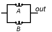
The first example is the AND gate, whose truth table is shown below, left. The Boolean AND function can be implemented with two switches, A and B, as shown below, right. If a power lead is connected to switch A, and a wire connects switches A and B, then both A and B have to be "on" in order for the output of the circuit to conduct electricity and provide power.
| INPUT | OUTPUT | |
|---|---|---|
| A | B | A AND B |
| 0 | 0 | 0 |
| 1 | 0 | 0 |
| 0 | 1 | 0 |
| 1 | 1 | 1 |
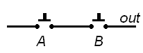
Switch circuit diagram for AND gate
OR gates
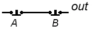
Another important arrangement is the OR gate, whose truth table is shown below, left.
An OR gate can be constructed from two switches, arranged so that if either switch is "on", the output will also be "on". Note that the output will still be on even if both switches are on.
| INPUT | OUTPUT | |
|---|---|---|
| A | B | A OR B |
| 0 | 0 | 0 |
| 1 | 0 | 1 |
| 0 | 1 | 1 |
| 1 | 1 | 1 |
Switch circuit diagram for OR gate
NOT gates
A simpler arrangement is the NOT gate, whose truth table is shown opposite.
This is a special switch that when pushed breaks the current when it is pressed. The normally-closed contact of a relay can be used for this purpose.
| INPUT | OUTPUT |
|---|---|
| A | NOT A |
| 0 | 1 |
| 1 | 0 |
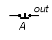
Switch circuit diagram for NOT gate
NAND and NOR gates
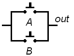
Using NOT gates, also called inverters, allows us to make alternate versions of the AND and OR gates, by virtue of De Morgan's Law. Note that the layout of the switches in the two circuits is swapped when we turn the switches "backwards". Also note how the output of the first pair controls the operation of the NOT gate.
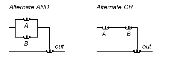
Switch diagram of alternate AND and OR gates
This may seem like an unnecessary complication, but in fact this is very useful. By removing the NOT gate from these alternate circuits, we create the so-called NAND (for NOT-AND) and NOR (for NOT-OR) gates.
NAND
| INPUT | OUTPUT | |
|---|---|---|
| A | B | A NAND B |
| 0 | 0 | 1 |
| 1 | 0 | 1 |
| 0 | 1 | 1 |
| 1 | 1 | 0 |
Switch circuit diagram of NAND gate
NOR
| INPUT | OUTPUT | |
|---|---|---|
| A | B | A NOR B |
| 0 | 0 | 1 |
| 1 | 0 | 0 |
| 0 | 1 | 0 |
| 1 | 1 | 0 |
Switch circuit diagram of NOR gate
XOR and XNOR gates
There exist two other 'basic' logic gates - XOR (exclusive-OR)and XNOR (exclusive-NOR).
| INPUT | OUTPUT | |
|---|---|---|
| A | B | A XOR B |
| 0 | 0 | 0 |
| 0 | 1 | 1 |
| 1 | 0 | 1 |
| 1 | 1 | 0 |
XOR is a 'stricter' version of the OR gate. Rather than allowing the output to be HIGH when either one or both of the inputs are HIGH, an XOR gate has a HIGH output only when only one input is HIGH. As such it has the truth table shown to the right. This can also be interpreted (for a two-input gate) as "HIGH output when the inputs are different".
| INPUT | OUTPUT | |
|---|---|---|
| A | B | A XNOR B |
| 0 | 0 | 1 |
| 1 | 0 | 0 |
| 0 | 1 | 0 |
| 1 | 1 | 1 |
XNOR is an inverted version of the XOR gate. As such it has the truth table shown to the right. This can also be interpreted as "HIGH output when the inputs are same".
The preceding simple logic gates can be combined to form more complicated boolean logic circuits. Logic circuits are often classified in two groups: combinatorial logic, in which the outputs are continuous-time functions of the inputs, and sequential logic, in which the outputs depend on information stored by the circuits as well as on the inputs.
Background
The simplest form of electronic logic is diode logic. This allows AND and OR gates to be built, but not inverters, and so is an incomplete form of logic. To build a complete logic system, valves or transistors can be used. The simplest family of logic gates using bipolar transistors is called resistor-transistor logic, or RTL. Unlike diode logic gates, RTL gates can be cascaded indefinitely to produce more complex logic functions. These gates were used in early integrated circuits. For higher speed, the resistors used in RTL were replaced by diodes, leading to diode-transistor logic, or DTL. It was then discovered that one transistor could do the job of two diodes in the space of one diode, so transistor-transistor logic, or TTL, was created. In some types of chip, to reduce size and power consumption still further, the bipolar transistors were replaced with complementary field-effect transistors (MOSFETs), resulting in complementary metal-oxide-semiconductor (CMOS) logic.
For small-scale logic, designers now use prefabricated logic gates from families of devices such as the TTL 7400 series invented by Texas Instruments and the CMOS 4000 series invented by RCA, and their more recent descendants. These devices usually contain transistors with multiple emitters, used to implement the AND function, which are not available as separate components. Increasingly, these fixed-function logic gates are being replaced by programmable logic devices, which allow designers to pack a huge number of mixed logic gates into a single integrated circuit. The field-programmable nature of programmable logic devices such as FPGAs has removed the 'hard' property of hardware; it is now possible to change the logic design of a hardware system by reprogramming some of its components, thus allowing the features or function of a hardware implementation of a logic system to be changed.
Electronic logic gates differ significantly from their relay-and-switch equivalents. They are much faster, consume much less power, and are much smaller (all by a factor of a million or more in most cases). Also, there is a fundamental structural difference. The switch circuit creates a continuous metallic path for current to flow (in either direction) between its input and its output. The semiconductor logic gate, on the other hand, acts as a high-gain voltage amplifier, which sinks a tiny current at its input and produces a low-impedance voltage at its output. It is not possible for current to flow between the output and the input of a semiconductor logic gate.
Another important advantage of standardised semiconductor logic gates, such as the 7400 and 4000 families, is that they are cascadable. This means that the output of one gate can be wired to the inputs of one or several other gates, and so on ad infinitum, enabling the construction of circuits of arbitrary complexity without requiring the designer to understand the internal workings of the gates.
In practice, the output of one gate can only drive a finite number of inputs to other gates, a number called the 'fanout limit', but this limit is rarely reached in the newer CMOS logic circuits, as compared to TTL circuits. Also, there is always a delay, called the 'propagation delay', from a change in input of a gate to the corresponding change in its output. When gates are cascaded, the total propagation delay is approximately the sum of the individual delays, an effect which can become a problem in high-speed circuits.
Logic levels
The two logic levels in binary logic circuits can be described as two voltage ranges, "zero" and "one", or "high" and "low". Each technology has its own requirements for the voltages used to represent the two logic levels, to ensure that the output of any device can reliably drive the input of the next device. Usually, two non-overlapping voltage ranges, one for each level, are defined. The difference between the high and low levels ranges from 0.7 volts in ECL logic to around 28 volts in relay logic.
Logic gates and hardware
NAND and NOR logic gates are the two pillars of logic, in that all other types of Boolean logic gates (i.e., AND, OR, NOT, XOR, XNOR) can be created from a suitable network of just NAND or just NOR gate(s). They can be built from relays or transistors, or any other technology that can create an inverter and a two-input AND or OR gate.
These functions can be seen in the table below. As you look at this table, start with the name of a gate and read across the table while you apply the following statement:

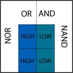
Basic Logic Functions
- OR: Any high in will create a high output
- NOR: Any high in will create a low output
- AND: Any low in will create a low output
- NAND: Any low in will create a high output
Logic gates are a vital part of many digital circuits, and as such, every kind is available as an IC. For examples, see the 4000 series of CMOS logic chips.
Symbols
There are two sets of symbols in common use, both now defined by ANSI/IEEE Std 91-1984 and its supplement ANSI/IEEE Std 91a-1991. The "distinctive shape" set, based on traditional schematics, is used for simple drawings and is quicker to draw by hand. It is sometimes unofficially described as "military", reflecting its origin if not its modern usage. The "rectangular shape" set, based on IEC 60617-12, has rectangular outlines for all types of gate, and allows representation of a much wider range of devices than is possible with the traditional symbols. The IEC's system has been adopted by other standards, such as EN 60617-12:1999 in Europe and BS EN 60617-12:1999 in the United Kingdom.
| Type | Distinctive shape | Rectangular shape |
|---|---|---|
| AND | 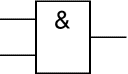
| |
| OR | 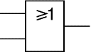
| |
| NOT | 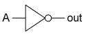 |
|
| In electronics a NOT gate is more commonly called an inverter. The circle on the symbol is called a bubble, and is generally used in circuit diagrams to indicate an inverted input or output. | ||
| NAND | 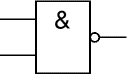
| |
| NOR | 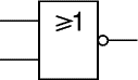
| |
| In practice, the cheapest gate to manufacture is usually the NAND gate. Additionally, Charles Peirce showed that NAND gates alone (as well as NOR gates alone) can be used to reproduce all the other logic gates.
Symbolically, a NAND gate can also be shown using the OR shape with bubbles on its inputs, and a NOR gate can be shown as an AND gate with bubbles on its inputs. This reflects the equivalency due to De Morgans law, but it also allows a diagram to be read more easily, or a circuit to be mapped onto available physical gates in packages easily, since any circuit node that has bubbles at both ends can be replaced by a simple bubble-less connection and a suitable change of gate. If the NAND is drawn as OR with input bubbles, and a NOR as AND with input bubbles, this gate substitution occurs automatically in the diagram (effectively, bubbles "cancel"). This is commonly seen in real logic diagrams - thus the reader must not get into the habit of associating the shapes exclusively as OR or AND shapes, but also take into account the bubbles at both inputs and outputs in order to determine the "true" logic function indicated. Two more gates are the exclusive-OR or XOR function and its inverse, exclusive-NOR or XNOR. The two input Exclusive-OR is true only when the two input values are different, false if they are equal, regardless of the value. If there are more than two inputs, the gate generates a true at its output if the number of trues’s at its input is odd ([1]). In practice, these gates are built from combinations of simpler logic gates. | ||
| XOR | 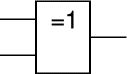
| |
| XNOR | 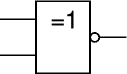
| |
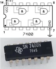
The 7400 chip, containing four NAND's. The two additional contacts supply power (+5 V) and connect the ground. It was a very popular chip, widely used by amateurs
Storage of bits
Related to the concept of logic gates (and also built from them) is the idea of storing a bit of information. The gates discussed up to here cannot store a value: when the inputs change, the outputs immediately react. It is possible to make a storage element either through a capacitor (which stores charge due to its physical properties) or by feedback. Connecting the output of a gate to the input causes it to be put through the logic again, and choosing the feedback correctly allows it to be preserved or modified through the use of other inputs. A set of gates arranged in this fashion is known as a "latch", and more complicated designs that utilise clocks (signals that oscillate with a known period) and change only on the rising edge are called edge-triggered "flip-flops". The combination of multiple flip-flops in parallel, to store a multiple-bit value, is known as a register.
These registers or capacitor-based circuits are known as computer memory. They vary in performance, based on factors of speed, complexity, and reliability of storage, and many different types of designs are used based on the application.
Three-state logic gates
Three-state, or 3-state, logic gates are a form of electronic logic gate in which the output has three possible states: high (H), low (L) and high-impedance (Z). The Z state exists merely to help the circuit designer and, unlike the H and L states, carries no information. This feature is used in circuits that have two or more logic outputs connected to a single logic input. A control circuit enables one output at a time depending on the logic function that is required, the other outputs being held in the Z state (also called 'disabled').
'Tri-state', a widely-used synonym of 'three-state', is a trademark of the National Semiconductor Corporation.
Miscellaneous
Logic circuits include such devices as multiplexers, registers, ALUs, and computer memory, all the way up through complete microprocessors which can contain more than a million gates. In practice, the gates are made from field effect transistors (FETs), particularly metal-oxide-semiconductor FETs (MOSFETs).
In reversible logic, Toffoli gates are used.
History and development
The earliest logic gates were made mechanically. Charles Babbage[[2]], around 1837, devised the Analytical Engine. His logic gates relied on mechanical gearing to perform operations. Electromagnetic relays were later used for logic gates. In 1891, Almon Strowger patented a device containing a logic gate switch circuit (Template:US patent). Strowger's patent was not in widespread use until the 1920s. Starting in 1898, Nikola Tesla [[3]]filed for patents of devices containing logic gate circuits (see List of Tesla patents). Eventually, vacuum tubes replaced relays for logic operations. Lee De Forest's modification, in 1907, of the Fleming valve can be used as AND logic gate. Claude E. Shannon introduced the use of Boolean algebra in the analysis and design of switching circuits in 1937. Walther Bothe, inventor of the coincidence circuit, got part of the 1954 Nobel prize in physics, for the first modern electronic AND gate in 1924.
See also
- Digital circuit
- Fanout
- Karnaugh map[[4]]
- List of Boolean algebra topics[[5]]
- Logic families [6]]
- NMOS[[7]]
- Race hazard[[8]]
- Venn diagram[[9]]
External links and references
- Symbols for logic gates. Twenty First Century Books, Breckenridge, CO.
- Tesla's invention of the AND logic gate. Twenty First Century Books, Breckenridge, CO.
- Wireless Remote Control and the Electronic Computer Logic Gate. Twenty First Century Books, Breckenridge, CO.
- Anderson, Leland I., "Nikola Tesla — Guided Weapons & Computer Technology". ISBN 0-9636012-5-3
- Bigelow, Ken, "How logic gates work internally (for several logic families)", play-hookey.com.
- C. E. Shannon, "A symbolic analysis of relay and switching circuits," Transactions American Institute of Electrical Engineers, vol. 57, pp. 713-723, March 1938.
- The International Electrotechnical Commission IEC[[10]] symbols are defined in IEC 60617-12 (1997-12), Graphical symbols for diagrams - Part 12: Binary logic elements
Further reading
- Bostock, Geoff, "Programmable logic devices : technology and applications". New York, McGraw-Hill, c1988. ISBN 0070066116
- Brown, Stephen D. et. al., "Field-programmable gate arrays". Boston, Kluwer Academic Publishers, c1992. The Kluwer international series in engineering and computer science. ISBN 0792392485
- Awschalom, D., D. Loss, and N. Samarth, "Semiconductor spintronics and quantum computation". Berlin, Springer, c2002. ISBN 3540421769